Beyond the Package: Unleashing Efficiency with Wafer-Level Packaging
In the relentless drive towards smaller, thinner, and more cost-effective electronics, the traditional approach of packaging individual integrated circuits (ICs) after dicing the wafer is undergoing a significant transformation. Enter Wafer-Level Packaging (WLP), a revolutionary methodology that shifts the packaging process to the wafer level before the individual dies are singulated. This paradigm shift offers a compelling array of advantages, making WLP a cornerstone of modern microelectronics, particularly for mobile, wearable, and IoT devices.
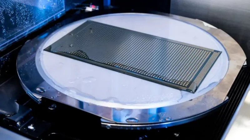
Imagine the conventional packaging process: a silicon wafer containing numerous chips is fabricated, tested, and then cut into individual dies. Each die is then picked and placed into a separate package, with wire bonds or other interconnects linking the chip to the package leads. WLP, however, flips this script. It involves performing key packaging steps – such as redistribution layers (RDLs), under-bump metallization (UBM), and even the formation of solder bumps – while the dies are still part of the entire wafer. Only after these wafer-level processes are complete is the wafer diced into individual packaged chips.
What makes this wafer-first approach so advantageous?
- Miniaturization and Thinning: One of the most significant benefits of WLP is the dramatic reduction in package size and thickness. Traditional packaging adds significant bulk around the die. WLP, particularly fan-in WLP, often results in a package that is essentially the same size as the die itself. This ultra-thin profile is crucial for sleek smartphones, compact wearables, and other space-constrained applications.
- Improved Electrical Performance: By eliminating the need for long wire bonds connecting the die to the package leads, WLP significantly reduces parasitic inductance and capacitance. This translates to improved signal integrity, faster operating speeds, and enhanced high-frequency performance – critical for demanding applications like 5G and advanced processors.
- Enhanced Thermal Performance: The direct connection of the die to the external environment facilitated by some WLP techniques, like flip-chip configurations, often leads to better heat dissipation. This allows devices to operate at higher power levels without overheating, improving reliability and performance.
- Lower Manufacturing Costs: Processing at the wafer level offers inherent economies of scale. Many packaging steps are performed simultaneously on hundreds or even thousands of dies, leading to higher throughput and lower per-unit costs compared to individually packaging each die.
- Increased Reliability: The shorter interconnects and the elimination of wire bonds in many WLP approaches can lead to improved mechanical and electrical reliability, making devices more robust and durable.
- Flexibility in Interconnect Density: WLP technologies like redistribution layers (RDLs) allow for finer pitch interconnections and more complex routing than traditional wire bonding, enabling higher input/output (I/O) counts and greater design flexibility. See also: Flex Rigid PCBs
Different Flavors of Wafer-Level Packaging:
The world of WLP encompasses several distinct technologies, each with its own strengths and applications:
- Fan-In WLP: This is the simplest form, where the package footprint is essentially the same size as the die. Interconnections are routed within the die area. It’s ideal for small, low I/O count devices.
- Fan-Out WLP: This technology allows for a package footprint that is larger than the die. Redistribution layers extend beyond the die area, enabling a higher number of I/O connections with larger pad pitches. Fan-out WLP is gaining popularity for high-performance mobile processors and application processors.
- Through-Silicon Via (TSV) Based WLP: TSVs are vertical interconnects etched through the silicon die, providing the shortest possible electrical paths and enabling 3D stacking of multiple dies. This is crucial for high-bandwidth memory (HBM) and advanced multi-chip modules.
Challenges and Considerations:
While WLP offers numerous advantages, it also presents certain challenges:
- Wafer Warpage: Processing entire wafers can introduce stress and lead to warpage, which can complicate subsequent handling and assembly processes.
- Known Good Die (KGD) Requirement: Since packaging occurs before dicing, ensuring that all dies on the wafer are functional (KGD) is crucial to avoid packaging defective chips and incurring unnecessary costs.
- Standardization: The wide variety of WLP technologies and processes can sometimes lead to a lack of standardization, making it challenging for designers and manufacturers.
- Infrastructure Investment: Implementing WLP requires specialized equipment and expertise, which can involve significant upfront investment.
The Future is Wafer-Level:
Despite these challenges, Wafer-Level Packaging is poised to play an increasingly dominant role in the future of microelectronics. As devices continue to shrink and demand higher performance, the efficiency, miniaturization, and cost benefits offered by WLP make it an indispensable technology. From the tiny sensors in IoT devices to the powerful processors in our smartphones and the high-bandwidth memory in advanced computing systems, WLP is quietly revolutionizing the way we package and integrate our increasingly sophisticated electronics. By thinking beyond the individual package and embracing the efficiency of wafer-scale processing, the industry is paving the way for a future of smaller, faster, and more powerful devices.
Ti potrebbe interessare:
Segui guruhitech su:
- Google News: bit.ly/gurugooglenews
- Telegram: t.me/guruhitech
- X (Twitter): x.com/guruhitech1
- Bluesky: bsky.app/profile/guruhitech.bsky.social
- GETTR: gettr.com/user/guruhitech
- Rumble: rumble.com/user/guruhitech
- VKontakte: vk.com/guruhitech
- MeWe: mewe.com/i/guruhitech
- Skype: live:.cid.d4cf3836b772da8a
- WhatsApp: bit.ly/whatsappguruhitech
Esprimi il tuo parere!
Ti è stato utile questo articolo? Lascia un commento nell’apposita sezione che trovi più in basso e se ti va, iscriviti alla newsletter.
Per qualsiasi domanda, informazione o assistenza nel mondo della tecnologia, puoi inviare una email all’indirizzo [email protected].
Scopri di più da GuruHiTech
Abbonati per ricevere gli ultimi articoli inviati alla tua e-mail.