
Why Is PCB Impedance Control Crucial
1. Introduction
In the relentless march of modern electronics, speed is paramount. From gigabit Ethernet to advanced microprocessors, signals are zipping across Printed Circuit Boards (PCBs) at ever-increasing frequencies. But with this speed comes a critical challenge : maintaining signal integrity. Imagine trying to have a clear conversation in a noisy room; high-speed signals face similar interference and degradation if not properly managed. This is where impedance control on a PCB becomes not just a best practice, but an absolute necessity.
Without precise impedance control, even minor mismatches can cause chaos: distorted waveforms, unexpected delays, signal reflections, and potentially corrupted data. These aren’t abstract risks; they are real -world problems that can lead to system malfunctions, reduced reliability, and costly design revisions. Whether you’re a seasoned PCB designer or an engineer looking to optimize your hardware, understanding the “why” and “how” of PCB impedance control is fundamental to crafting reliable, high-performance electronic devices.
2. What is Impedance in a PCB?
To grasp the significance of impedance control, we first need to define impedance itself. In simple terms, impedance (measured in Ohms, Ω) is the total opposition a circuit presents to an alternating current (AC). Unlike simple resistance, which only accounts for energy dissipation, impedance also includes the effects of capacitance and inductance, which store and release energy. For a DC current, a wire is just a resistor. But when dealing with high-frequency AC signals, PCB traces begin to behave less like simple wires and more like transmission lines .
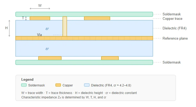
In a high-speed PCB, a transmission line is formed by a trace and its adjacent reference plane (either a ground or power plane). The physical dimensions of this trace (width, thickness), its proximity to the reference plane, and the dielectric material separating them all contribute to what’s known as the characteristic impedance. This characteristic impedance is a critical parameter that determines how signals propagate along the trace without reflections or distortion. When the signal frequency becomes high enough (generally above 100 MHz, though this threshold varies), the distributed capacitance and inductance along the trace become significant, making impedance a crucial design parameter rather than just a byproduct.
3. Why is Impedance Control Critical for High-Speed Designs?
The primary purpose of impedance control is to ensure optimal signal integrity. In high-speed circuits, signals travel as electromagnetic waves. If these waves encounter a sudden change in impedance along their path—for example, from a driver to a trace, from a trace to a via, or from a trace to a receiver—a portion of the signal energy will be reflected back towards the source. These signal reflections can cause several detrimental effects:
- Signal Distortion: Reflections superimpose on the original signal, altering its shape and potentially making it unrecognizable to the receiving component. This can lead to false triggering, bit errors, and system instability.
- Crosstalk: Reflections can radiate energy, inducing unwanted signals onto adjacent traces. This crosstalk becomes more pronounced in uncontrolled impedance environments, degrading the performance of neighboring signals.
- Timing Errors: Reflections can cause signal rise and fall times to become slower or faster, altering the precise timing required for synchronized digital circuits. This leads to setup and hold time violations, resulting in unreliable operation.
- Electromagnetic Interference (EMI ): Uncontrolled impedance can lead to ringing and oscillations, which generate unwanted electromagnetic radiation. This EMI can interfere with other components on the board or even external devices, causing compliance issues.
- Reduced Data Rates: Ultimately , these issues limit the maximum frequency and data rate that a PCB can reliably support. For modern applications requiring high bandwidth, controlled trace impedance is non-negotiable.
By carefully controlling the characteristic impedance of traces, designers can achieve impedance matching throughout the signal path, from source to load. This minimizes reflections, ensuring that the maximum amount of signal energy reaches its destination with minimal distortion, thus maintaining the integrity and reliability of the high-speed signals.
4. Key Factors Influencing PCB Impedance
The characteristic impedance of a PCB trace is not an arbitrary value; it’s determined by a precise interplay of several physical and material properties. Understanding these factors is crucial for designing and manufacturing PCBs with consistent trace impedance.
| Factor | Description | Impact on Impedance |
| Trace Width | The lateral dimension of the conductive copper trace. | Wider traces generally lower impedance, while narrower traces increase it. |
| Trace Thickness | The vertical dimension of the copper trace (e.g., 1 oz, 2 oz copper). | Thicker traces generally lower impedance. |
| Dielectric Constant (εr) | A material property of the insulating (dielectric) layer between the trace and its reference plane. | Higher dielectric constant (εr) lowers impedance. Lower εr increases impedance. |
| Dielectric Height (H) | The thickness of the insulating layer between the trace and its reference plane. | Larger dielectric height increases impedance. Smaller height lowers it. |
| Distance to Reference Plane | The vertical distance from the trace to its nearest ground or power plane. | Closer proximity to a reference plane (smaller H) lowers impedance. |
| Trace Geometry | Whether the trace is a microstrip (outer layer) or stripline (inner layer), or coplanar. | Different geometries have different impedance formulas and sensitivities to other factors. |
| Soldermask Thickness/εr | The thickness and dielectric constant of the soldermask layer over a surface trace. | Can slightly lower the impedance of a micro strip trace due to its dielectric properties. |
Due to the sensitivity of these parameters, even small variations during manufacturing can significantly affect the final impedance. This is why strict process control and material consistency are vital for manufacturers offering PCB impedance control capabilities.
5. Designing for Controlled Impedance
Implementing impedance control in PCB routing requires careful planning and collaboration between the designer and the PCB manufacturer. The process typically involves:
1. Defining Impedance Requirements: Identify which signals require controlled impedance and their target impedance values (e.g ., 50 Ohms for RF, 100 Ohms differential for high-speed data).
2. Layer Stackup Definition: Work with the PCB fabricator to define a layer stackup that allows for specific dielectric heights and materials to achieve the target impedances. The stackup dictates the available reference planes and dielectric thicknesses.
3. Impedance Calculation: Utilize specialized impedance calculators (often built into PCB design software or provided by manufacturers) to determine the precise trace width and spacing required for the desired impedance, given the chosen stackup and materials. These tools use electromagnetic field solvers to accurately model the transmission lines.
4. Routing Guidelines: Adhere to strict routing guidelines:
- Maintain consistent trace width and spacing for differential pairs.
- Ensure unbroken reference planes beneath controlled impedance traces.
- Minimize the use of vias or optimize their design to avoid impedance discontinuities.
- Route traces away from noisy areas and avoid sharp 90-degree bends.
5. Design Verification: Use post-layout simulation tools (like Signal Integrity (SI) analysis software) to verify the impedance profile and predict signal behavior before manufacturing.
6. Manufacturing Tolerances: Be aware that manufacturing processes have tolerances. Designers should communicate target impedances and acceptable tolerances to the fabricator, who will then adjust their process parameters (e.g., etching time, material thickness) to meet these specifications. Manufacturers often perform Time Domain Reflectometry (TDR) testing to verify actual impedance values on test coupons.
Effective communication with your PCB manufacturer is paramount . They possess critical data on material properties and process capabilities that directly impact the impedance values you can achieve.
6. Common Transmission Line Structures
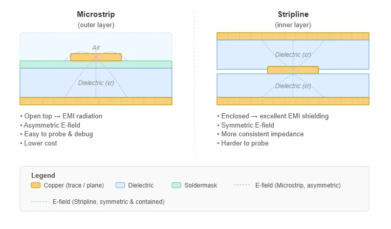
To achieve controlled impedance, designers primarily use two types of transmission line structures:
Microstrip
A microstrip is a trace routed on an outer layer of the PCB, separated from an adjacent internal ground or power plane by a dielectric material.
· Advantages: Easier to fabricate, good heat dissipation, accessible for probing.
· Disadvantages: More susceptible to EMI radiation and crosstalk due to its open structure. The top surface soldermask can also influence its impedance.
· Typical Use: Often used for single-ended signals and moderately high-speed differential pairs where cost or accessibility is a factor.
Stripline
A stripline is a trace routed on an inner layer, sandwiched between two reference planes (usually ground planes).
- Advantages: Excellent EMI shielding due to being fully embedded, less susceptible to crosstalk, more consistent impedance.
- Disadvantages: Harder to fabricate (requiring more precise layer alignment), less accessible for debugging, and poorer heat dissipation.
- Typical Use: Preferred for very high-speed differential pairs and sensitive analog signals where maximum signal integrity and EMI suppression are critical.
Coplanar Waveguide
A less common but effective structure, a coplanar waveguide involves a central trace with ground planes running parallel on the same layer, providing a tighter field confinement and often used in RF applications. These can be on outer layers (grounded coplanar waveguide) or inner layers (embedded coplanar waveguide).
7. Applications of Impedance Control
The need for impedance control spans across a wide range of electronic applications, becoming increasingly vital as operating frequencies rise:
- High-Speed Digital Interfaces: Modern processors, FPGAs, and ASICs rely on high -speed interfaces like DDR (DDR3, DDR4, DDR5), PCIe, USB 3.0/4.0, HDMI, and Ethernet (10GBASE-T and beyond). These interfaces demand tight impedance control to prevent data corruption and ensure reliable communication at gigabit speeds.
- Radio Frequency (RF) and Microwave Circuits : In RF applications (e.g., Wi-Fi, Bluetooth, cellular communications), trace impedance matching is absolutely critical for efficient power transfer between components, antenna matching, and minimizing signal loss and reflections. Common impedances here are 50 Ω for single-ended and 100 Ω for differential signals.
- Memory Subsystems: Memory buses often involve many parallel data lines running at high frequencies. Controlled impedance ensures that all data lines have similar propagation delays, preventing skew and allowing for synchronous operation.
- Video and Display Interfaces: Standards like HDMI, DisplayPort, and LVDS require precise impedance control for their high-speed differential pairs to ensure clear, high-resolution video transmission without artifacts.
· Data Centers and Networking Equipment: With vast amounts of data moving at extremely high rates, the backplanes and line cards in servers, switches, and routers heavily rely on controlled trace impedance to maintain data integrity and system reliability.
Essentially, any system operating with signal rise times faster than approximately six times the trace propagation delay is a candidate for impedance control. As electronic devices become smaller, faster, and more complex , the role of impedance control in a PCB will only grow in importance.
8. FAQ
Q1: What is the difference between resistance and impedance in a PCB?
A: Resistance is the opposition to direct current (DC) flow and dissipates energy as heat. Impedance is the opposition to alternating current (AC) flow and includes both resistance and reactive components (capacitance and inductance). In high-speed PCBs, traces act as transmission lines, where impedance, not just resistance, dictates signal behavior.
Q2: How does a PCB manufacturer verify impedance control?
A: PCB manufacturers typically use a technique called Time Domain Reflectometry (TDR). A TDR instrument sends a fast rise-time pulse down a test coupon (a small trace fabricated on the same panel as your PCB) and measures any reflections. The reflected waveform reveals the impedance profile along the trace, allowing the manufacturer to confirm that the impedance meets specified tolerances.
Q: Can impedance control be applied to every trace on a PCB?
A: While theoretically possible, it’s generally not necessary or cost-effective. Impedance control is specifically critical for high-speed signals, RF signals, and sensitive analog signals where signal integrity is paramount. Lower speed or DC traces do not require controlled impedance, allowing designers to save on manufacturing costs and design complexity.
9. Summary
In the realm of high -speed electronics, impedance control on a PCB is a foundational principle for achieving reliable performance. It moves beyond simple resistance, acknowledging that high-frequency signals transform traces into complex transmission lines. By maintaining a consistent characteristic impedance throughout a signal path, designers effectively prevent detrimental signal reflections, minimize crosstalk , and mitigate timing errors that can corrupt data or cause system instability.
Key factors like trace width, dielectric constant, and distance to the reference plane all play a crucial role, necessitating precise design calculations and tight manufacturing tolerances. Whether dealing with complex memory interfaces or sensitive RF circuits, understanding and implementing impedance control in PCB routing is indispensable for ensuring the signal integrity and overall functionality of modern electronic devices.
Ti potrebbe interessare:
Segui guruhitech su:
- Google News: bit.ly/gurugooglenews
- Telegram: t.me/guruhitech
- Facebook: facebook.com/guruhitechfb
- Instagram: instagram.com/guruhitech_official/
- X (Twitter): x.com/guruhitech1
- Bluesky: bsky.app/profile/guruhitech.bsky.social
- Rumble: rumble.com/user/guruhitech
- VKontakte: vk.com/guruhitech
- MeWe: mewe.com/i/guruhitech
- Skype: live:.cid.d4cf3836b772da8a
- WhatsApp: bit.ly/whatsappguruhitech
Esprimi il tuo parere!
Ti è stato utile questo articolo? Lascia un commento nell’apposita sezione che trovi più in basso e se ti va, iscriviti alla newsletter.
Per qualsiasi domanda, informazione o assistenza nel mondo della tecnologia, puoi inviare una email all’indirizzo [email protected].
Scopri di più da GuruHiTech
Abbonati per ricevere gli ultimi articoli inviati alla tua e-mail.