
High-Frequency PCB Design Guide: Materials, Stackup, Layout & Manufacturing
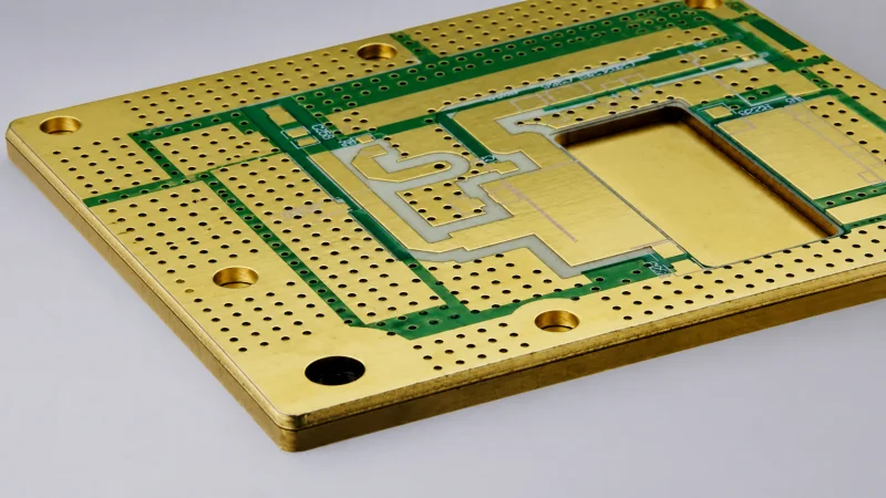
If you’ve ever watched a 28 GHz 5G antenna array fail on the first prototype, you already know the problem. The design looked right in simulation, the schematic was clean, but the board itself destroyed your signal. High-frequency PCB design is fundamentally different from digital board design — every trace is a transmission line, every via is a parasitic element, and the board material itself becomes an active part of the circuit.
What is High-Frequency PCB Design?
A PCB enters the “high-frequency” domain when the signal wavelength becomes comparable to the physical dimensions of traces, vias, and components on the board. This typically happens above 1 GHz, where the wavelength in FR-4 shrinks to roughly 6–8 cm — short enough that a poorly placed via or an unmatched stub can cancel your signal completely.
At these frequencies, standard design rules break down. A trace isn’t just a wire — it’s a transmission line with characteristic impedance, propagation delay, and frequency-dependent loss. A ground plane isn’t just a reference — it’s the return path that must be continuous for the signal to propagate cleanly.
Design Challenges at High Frequencies
| Challenge | Impact | Typical Cause |
| Impedance mismatch | Signal reflections, power loss | Wrong trace width, incorrect dielectric spacing |
| Insertion loss | Weak signal at receiver | High Df material, rough copper, long trace length |
| Crosstalk | Unwanted coupling between channels | Insufficient trace spacing, lack of isolation |
| Via stub resonance | Notch filter effect at specific frequencies | Unused via barrel length acts as resonant stub |
| Skin effect losses | Higher resistance at RF frequencies | Rough copper surface finish |
| EMI / radiation | Failed compliance testing | Uncontrolled return paths, poor shielding |
Frequency Ranges and Their Design Complexity
| Frequency Range | Typical Applications | Material Requirement |
| 1–3 GHz | Cellular, GPS, Wi-Fi | High-Tg FR-4 or Rogers RO4350B |
| 3–10 GHz | 5G sub-6, radar, satellite | Rogers RO4003C, RO4350B |
| 10–30 GHz | 5G mmWave, automotive radar | Rogers RO3003, RT/duroid 5880 |
| 30–100+ GHz | Satellite, defense, test equipment | RT/duroid 5880, ceramic-filled PTFE |
Material Selection for High-Frequency PCBs
Material choice is the single most important decision in high-frequency PCB design. The wrong substrate can make an otherwise perfect design unusable above a few gigahertz.
Why FR-4 Fails at High Frequencies
Standard FR-4 has a dissipation factor (Df) of approximately 0.02–0.025 at 1 GHz. This doesn’t sound terrible until you calculate the loss: at 10 GHz, FR-4’s dielectric losses alone can exceed 3 dB per inch of trace — meaning half your signal power disappears in every inch of board. Combine this with the material’s ±10% dielectric constant (Dk) variation and you have no way to guarantee impedance control across production batches.
High-Frequency Material Comparison
| Material | Dk (at 10 GHz) | Df (at 10 GHz) | Cost vs FR-4 | Typical Use |
| Standard FR-4 | 4.2–4.8 ±10% | 0.020–0.025 | 1× | Below 1 GHz only |
| High-Tg FR-4 | 4.2–4.5 ±8% | 0.015–0.020 | 1.5–2× | Up to 3 GHz, moderate loss OK |
| Rogers RO4350B | 3.48 ±0.05 | 0.0037 | 4–5× | 5G, automotive radar, base stations |
| Rogers RO4003C | 3.38 ±0.05 | 0.0027 | 5–6× | Higher-performance RF, LNA |
| Rogers RO3003 | 3.00 ±0.04 | 0.0013 | 6–8× | Millimeter-wave radar, 77 GHz |
| RT/duroid 5880 | 2.20 ±0.02 | 0.0009 | 8–12× | Satellite, ultra-low loss, >30 GHz |
Selecting a Rogers PCB Manufacturer
Not all fabrication shops can process high-frequency materials properly. Rogers laminates require specific drilling parameters, plasma desmear treatment, and controlled lamination cycles that standard FR-4 lines simply don’t support.
When evaluating a Rogers PCB manufacturer, look for three things: documented process control for PTFE-based materials, impedance tolerance verification with TDR reports, and material traceability back to Rogers lot certificates. A shop that treats RO4350B the same as standard FR-4 will produce boards with unreliable impedance and poor plated through-hole reliability.
For prototype and mid-volume production, the sweet spot is a manufacturer who runs the full Rogers stack — RO4003C, RO4350B, RT/duroid 5880, and RO3003 — with dedicated process lines and the engineering team to review high-frequency stackups before fabrication.
Impedance Control: The Foundation of High-Frequency Design
At high frequencies, every signal trace must have a controlled characteristic impedance. The two most common targets are 50Ω single-ended and 100Ω differential.
Microstrip vs Stripline
| Parameter | Microstrip | Stripline |
| Layer | Outer (top or bottom) | Inner, between two reference planes |
| Impedance range | 30–120Ω | 40–100Ω |
| Loss | Lower (no dielectric on top) | Higher (dielectric on both sides) |
| Shielding | Poor (top surface exposed) | Excellent (planes above and below) |
| Crosstalk | Higher | Lower |
| Manufacturing | Easier, wider traces | Harder, tighter tolerances |
Trace Width Calculation Guide
For 50Ω microstrip on Rogers RO4350B (Dk 3.48):
| Substrate Thickness | Copper Weight | Approx Trace Width |
| 8 mil (0.203 mm) | 0.5 oz | 13–14 mil |
| 10 mil (0.254 mm) | 0.5 oz | 17–18 mil |
| 12 mil (0.305 mm) | 0.5 oz | 20–22 mil |
| 20 mil (0.508 mm) | 1 oz | 37–40 mil |
| 31 mil (0.787 mm) | 1 oz | 58–62 mil |
Note: These are approximations. Always use a field solver (Polar Si9000, Keysight ADS, or your EDA tool’s built-in calculator) with the manufacturer’s specific prepreg and core stackup data.
Factors That Affect Impedance
- Dielectric constant: Lower Dk means wider traces for the same impedance — which is actually beneficial, because wider traces have lower conductor loss.
- Trace width tolerance: A ±0.5 mil variation can shift impedance by ±1–2Ω. Specify tighter tolerances for critical RF traces.
- Dielectric height variation: Prepreg thickness after lamination varies. Stackup design must account for the manufacturer’s standard materials.
- Solder mask: Solder mask has its own Dk (~3.5–4.0), and its presence on microstrip traces can lower impedance by 2–5Ω at high frequencies. Many RF designs strip the solder mask from critical transmission lines.
Stackup Design for High-Frequency PCBs
A well-designed stackup is the backbone of any high-frequency PCB. The goal is to provide consistent reference planes, controlled dielectric spacing, and adequate isolation between signal layers.
Stackup Guidelines
- High-speed signals on outer layers: Microstrip on top or bottom for lowest loss and easiest testing.
- Stripline for sensitive signals: Buried in inner layers between ground planes for maximum isolation.
- No split ground planes: Any slot or gap in the reference plane under a high-frequency trace creates an impedance discontinuity and a return path problem.
- Symmetry matters: Balanced copper distribution prevents warpage during lamination — especially important for Rogers materials with different CTE than FR-4.
Recommended 4-Layer High-Frequency Stackup
| Layer | Function | Material | Target Thickness |
| L1 | RF signals, 50Ω microstrip | Copper 1 oz | — |
| Prepreg | RO4450F or 2116 | 5–8 mil | |
| L2 | Ground (continuous) | Copper 1 oz | — |
| Core | Rogers RO4350B | 20–31 mil | |
| L3 | Power / DC signals | Copper 1 oz | — |
| Prepreg | FR-4 2116 | 5–8 mil | |
| L4 | Control / digital signals | Copper 1 oz | — |
Recommended 6-Layer High-Frequency Stackup
| Layer | Function | Material | Target Thickness |
| L1 | RF microstrip | Copper 0.5 oz | — |
| Prepreg | Rogers 2929 bondply | 4 mil | |
| L2 | Ground | Copper 0.5 oz | — |
| Core | Rogers RO4350B | 10 mil | |
| L3 | Stripline RF or digital | Copper 0.5 oz | — |
| Prepreg | RO4450F | 10 mil | |
| L4 | Ground | Copper 0.5 oz | — |
| Core | Rogers RO4350B | 10 mil | |
| L5 | Power / control | Copper 0.5 oz | — |
| Prepreg | Rogers 2929 bondply | 4 mil | |
| L6 | RF microstrip or digital | Copper 0.5 oz | — |
Hybrid stacks (Rogers cores + FR-4 prepregs for non-critical layers) are common to balance cost and performance. The RF layers use Rogers materials, while power and low-speed digital layers use standard FR-4.
PCB Layout Techniques for High-Frequency Signals
The layout phase is where good design practice meets practical manufacturing reality. These techniques apply regardless of whether you’re using FR-4 or Rogers materials.
Trace Geometry Rules
- 45° chamfered bends: Never use 90° corners on RF traces. The abrupt change in trace width creates a capacitance discontinuity and reflects signal energy. Use two 45° bends or rounded arcs instead.
- Minimize trace discontinuities: Transitioning from a wide trace to a narrow one (or vice versa) creates impedance mismatch. Use tapered transitions when changing widths.
- Keep RF traces short: Every millimeter of trace adds insertion loss. Place RF components as close together as routing allows.
- Avoid right-angle bends: At high frequencies, the outer edge of a 90° corner carries more current density, increasing radiation and reflection.
Isolation Techniques
| Isolation Method | Typical Isolation | Application |
| Air gap (no copper) | 15–25 dB | Adjacent traces same layer |
| Copper guard trace with ground vias | 30–45 dB | RF-to-RF isolation |
| Via fence (row of grounded vias) | 40–60 dB | RF block to RF block isolation |
| RF shielding can (metal enclosure) | 50–80 dB | Sensitive sections, VCO, LNA |
Ground Plane Design
- Never split a ground plane under an RF trace. Return current flows on the plane directly under the trace — any gap forces current around it, increasing inductance and causing radiation.
- Use generous ground fill on all signal layers. Stitch ground fills on outer layers to the internal ground plane every λ/8 or closer.
- Avoid “islands” of copper that are not grounded. Floating copper acts as a parasitic antenna.
Component Placement
- Place RF components first, then digital/power components. Group sections by function.
- Separate RF, analog, and digital sections on the board. Use physical distance and ground isolation.
- Orientation matters: Align RF components in the same orientation when possible to simplify trace routing and minimize bends.
- Decoupling capacitors must be placed as close as possible to the IC power pins. At high frequencies, the inductance of even 1 mm of trace between capacitor and pin can degrade decoupling performance.
Common Mistakes in High-Frequency PCB Design
Even experienced RF engineers make these mistakes. Here are the most common ones we see during DFM review.
Mistake 1: Using FR-4 above 3 GHz. The loss is too high, and the Dk variation makes impedance control impossible. Switch to Rogers RO4003C or RO4350B.
Mistake 2: Routing over a split ground plane. This creates an immediate return path discontinuity — your simulated and measured performance will differ dramatically.
Mistake 3: Ignoring via stubs. A via stub that’s 20 mil long resonates at approximately 60 GHz — which might be above your operating frequency. But a 40 mil stub resonates at 30 GHz, right in the 5G mmWave band.
Mistake 4: Specifying ±5% impedance without verifying the manufacturer’s capability. Not all shops can hold ±5% on Rogers materials in volume. Confirm capability before ordering.
Mistake 5: Forgetting solder mask effects. A microstrip design that calculates 50Ω without solder mask will measure 46–48Ω after fabrication with mask.
Mistake 6: Using standard HASL finish. The rough surface of HASL dramatically increases conductor losses at high frequencies due to the skin effect. Always specify ENIG or immersion silver for RF boards.
Frequently Asked Questions
What frequency range is considered “high-frequency” for PCB design?
Typically, designs operating above 1 GHz are considered high-frequency. At these frequencies, transmission line effects become dominant — trace lengths are no longer electrically short, and impedance control becomes mandatory. Many design guides set 1 GHz as the threshold, but in practice, careful layout is beneficial above 500 MHz for long traces.
Can I use FR-4 for high-frequency PCBs?
FR-4 can work up to approximately 1–2 GHz for short trace lengths (under a few inches). Above 2 GHz, the dielectric losses (Df ~0.02) become prohibitive, and the ±10% Dk variation makes reliable impedance control impossible without large margins. For designs above 3 GHz, Rogers RO4000 series or equivalent high-frequency laminates are strongly recommended.
What is back-drilling and when do I need it?
Back-drilling removes the unused stub portion of a plated through-hole via after the board is fabricated. This eliminates the resonant stub effect that can create a notch filter at specific frequencies. Back-drilling is recommended for any via carrying RF signals above 3 GHz and is essential above 10 GHz.
What impedance tolerance should I specify?
For standard RF designs (up to 10 GHz), ±10% is the commercial standard and achievable by most manufacturers. For 5G, radar, and high-performance designs (10–30 GHz), specify ±5% — this requires a manufacturer with tight process control and TDR verification. Also for millimeter-wave designs above 30 GHz, ±3% is sometimes required but should be discussed with your manufacturer first.
How do I choose between microstrip and stripline?
Microstrip offers lower loss and easier testing, making it preferred for RF output stages and antenna feeds. Stripline provides better isolation and shielding, making it the right choice for sensitive receiver paths and signals that must cross the board without picking up noise. Many designs use both: microstrip on outer layers for RF interfaces, stripline on inner layers for distribution.
What surface finish is best for high-frequency PCBs?
ENIG and immersion silver are the most practical choices for high-frequency designs. They provide smooth, planar surfaces that minimize skin effect losses. ENEPIG is even better for millimeter-wave applications but costs more. Avoid HASL for any RF trace that carries signals above 1 GHz — the rough surface finish adds measurable insertion loss.
How does solder mask affect high-frequency performance?
Solder mask has its own dielectric constant (3.3–4.0) and dissipation factor (0.02–0.03). When applied over microstrip traces, it effectively adds a lossy dielectric layer on top that lowers impedance by 2–5Ω and increases insertion loss. For critical RF traces above 10 GHz, removing the solder mask (specifying a mask opening in your Gerber layers) is standard practice.
Why do I need a turnkey PCB assembly partner for high-frequency boards?
High-frequency boards combine demanding material processing (Rogers laminates, PTFE), tight impedance tolerances, and complex assembly requirements. A turnkey PCB assembly partner with in-house RF experience reviews your stackup and layout for manufacturing issues before production, coordinates material procurement with fabrication, ensures compatible surface finishes, and tests the assembled boards. This single-point accountability catches problems that would otherwise surface as separate finger-pointing between a board fabricator, an assembly house, and a component distributor.
Conclusion
Start with material selection: choose the right Rogers laminate for your frequency band, pair it with a Rogers PCB manufacturer that has documented process control for PTFE-based materials. Design your stackup with continuous ground planes and controlled dielectric spacing. Use back-drilled vias for any RF signal path. Verify your design with TDR and VNA measurements before committing to volume production.
For practical implementation, partner with a manufacturer that offers end-to-end service — from DFM feedback on the high-frequency stackup through turnkey PCB assembly and RF testing. The engineering time saved by having one team review the entire manufacturing flow is substantial, and the confidence gained from verified impedance reports and tested assemblies is worth even more.
Ti potrebbe interessare:
Segui guruhitech su:
- Google News: bit.ly/gurugooglenews
- Telegram: t.me/guruhitech
- Facebook: facebook.com/guruhitechfb
- Instagram: instagram.com/guruhitech_official/
- X (Twitter): x.com/guruhitech1
- Bluesky: bsky.app/profile/guruhitech.bsky.social
- Rumble: rumble.com/user/guruhitech
- VKontakte: vk.com/guruhitech
- MeWe: mewe.com/i/guruhitech
- Skype: live:.cid.d4cf3836b772da8a
- WhatsApp: bit.ly/whatsappguruhitech
Esprimi il tuo parere!
Ti è stato utile questo articolo? Lascia un commento nell’apposita sezione che trovi più in basso e se ti va, iscriviti alla newsletter.
Per qualsiasi domanda, informazione o assistenza nel mondo della tecnologia, puoi inviare una email all’indirizzo [email protected].
Scopri di più da GuruHiTech
Abbonati per ricevere gli ultimi articoli inviati alla tua e-mail.