
HDI PCB Manufacturer: What to Look for Before You Place an Order
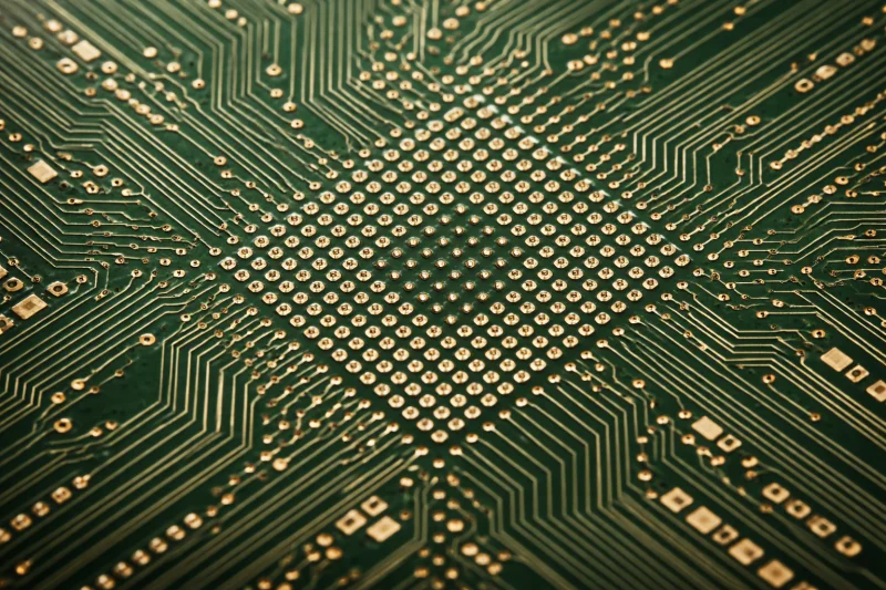
Choosing the right HDI PCB manufacturer is one of the most critical decisions in a high-density interconnect project. HDI boards are far more complex than standard multilayer PCBs. They require advanced technologies such as laser drilling, sequential lamination, microvia plating, and fine-line imaging, all of which demand specialized equipment and experienced engineering teams. Manufacturers without true HDI capability may accept your design files but fail to deliver boards that meet reliability and performance requirements.
This guide explains what HDI PCB manufacturing involves, which capabilities you must verify before placing an order, and how design decisions impact manufacturing success.
What HDI PCB Manufacturing Involves
HDI stands for High Density Interconnect, referring to PCBs designed with smaller vias, finer traces, and increased routing density. Compared to conventional boards, HDI PCBs allow more components and functionality within a compact area.
Key features of HDI boards include:
- Microvias – very small laser-drilled vias, typically 100 micrometers or less in diameter
- Blind vias – connect outer layers to inner layers without passing through the entire board
- Buried vias – connect internal layers only
- Sequential lamination – builds the board layer by layer to achieve high routing density
These technologies allow designers to place components closer together and route signals more efficiently, improving signal integrity and reducing board size.
HDI boards are widely used in smartphones, automotive electronics, medical devices, telecommunications systems, and high-performance computing applications.
HDI Board Types and Stack-up Structures
Commonly, HDI boards are classified by their stack-up structure:
1+N+1 Structure
One microvia layer is added to each side of the core. This is the most common HDI configuration, used in consumer electronics where moderate density improvements are required.
2+N+2 Structure
Two build-up layers are added to each side of the core. This structure supports higher routing density and is often used for processors with high pin-count BGAs.
Any-layer HDI
Each layer can connect using microvias. This design offers maximum routing flexibility and is used in advanced applications such as smartphone motherboards and compact computing modules.
Via in Pad
Microvias are drilled directly into component pads, enabling routing for extremely fine-pitch BGAs (0.4 mm pitch or below). The vias are filled with copper or epoxy and planarized to create a flat surface for soldering.
Manufacturers like FastTurn PCB support HDI stack-ups with up to 18 build-up layers and 32 total layers, enabling both prototype and high-volume production.
The HDI PCB Manufacturing Process
HDI PCB production involves multiple precise steps:
- Core Preparation
Inner layers are imaged using Laser Direct Imaging (LDI), enabling fine trace widths below 3 mil. Copper is etched to form circuit patterns and inspected for accuracy. - Build-up Layer Lamination
Thin dielectric material is laminated onto the core under controlled pressure and temperature. - Laser Drilling
Microvias are created using laser drilling technology to achieve high precision and small diameters. - Via Metallization
Microvias are plated with copper to create electrical connections between layers. Via-in-pad structures are filled and planarized for component mounting. - Outer Layer Imaging
Circuit patterns are imaged and etched onto each build-up layer using high-resolution LDI technology. - Sequential Build-up
Additional layers are added through repeated lamination, drilling, and plating cycles. - Surface Finish
Final layers receive soldermask and surface finishes such as ENIG or HASL to protect copper and ensure solderability. - Testing and Inspection
Boards undergo automated optical inspection (AOI), electrical testing, impedance verification, and X-ray inspection for buried vias.
Manufacturing Specifications to Verify
Before selecting an HDI PCB manufacturer, confirm these production capabilities:
- Minimum trace width and spacing: typically 2.5–3 mil
- Minimum microvia diameter: around 100 micrometers
- Maximum layer count supported
- Via fill and surface planarity for via-in-pad structures
- Controlled impedance tolerance (±5 ohms or ±10%)
- Layer-to-layer alignment accuracy
- Supported materials, including high Tg laminates and low-loss dielectrics
Request documentation, cross-section samples, or production examples to confirm actual capability rather than relying on marketing claims.
Design Decisions That Affect Manufacturing Success
Certain design choices significantly impact manufacturing yield, cost, and reliability:
Stacked vs Staggered Microvias
Stacked microvias save space but increase manufacturing complexity. Staggered vias are easier to produce and often provide better reliability.
Trace Width and Spacing
Design traces slightly wider than the minimum capability whenever possible. This improves yield and reduces cost.
Via in Pad Usage
Via in pad is necessary for very fine-pitch components but increases process complexity. Use only when required.
Impedance Control
High-speed signals require controlled impedance traces. Include impedance specifications and test coupons in your design files.
Board Thickness
Ensure through-hole aspect ratios remain within acceptable limits to maintain reliable plating quality.
Industries Using HDI PCB Technology
HDI PCBs are essential in applications requiring compact size and high performance:
- Smartphones and wearable devices
- Automotive electronics and ADAS systems
- Servers and AI accelerators
- Medical diagnostic equipment
- Aerospace and defense electronics
Questions to Ask an HDI PCB Manufacturer
Before placing an order, ask suppliers:
- Can you provide cross-section samples of microvias?
- What imaging technology is used for fine traces?
- What is your layer alignment tolerance?
- Which certifications do you hold (ISO, IPC, UL)?
- What is your prototype turnaround time?
Manufacturers with genuine HDI capability can provide detailed answers supported by real production data.
How FastTurn PCB Supports HDI Projects
FastTurn PCB has produced HDI boards since 2015 for customers in medical, automotive, telecommunications, and consumer electronics industries. Their manufacturing capabilities include:
- Microvias down to 100 micrometers
- Trace width and spacing down to 2.5 mil
- Up to 18 HDI build-up layers
- Via in pad with high surface planarity
- Controlled impedance within ±5 ohms
Each project begins with a Design for Manufacturability (DFM) review to identify potential issues before production starts. This process improves yield and reduces development time.
Conclusion
HDI PCB manufacturing requires specialized equipment, advanced process control, and experienced engineering teams. When choosing a manufacturer, verify real production capability through documentation, cross-sections, and technical specifications.
To get a free DFM review and quote for your next HDI design, visit HDI PCB manufacturer services at FastTurn PCB and upload your Gerber files for a same-day engineering review.
Scopri di più da GuruHiTech
Abbonati per ricevere gli ultimi articoli inviati alla tua e-mail.